Signal and Power Integrity
Welcome to Electromagnetic Compatibility LAB
-
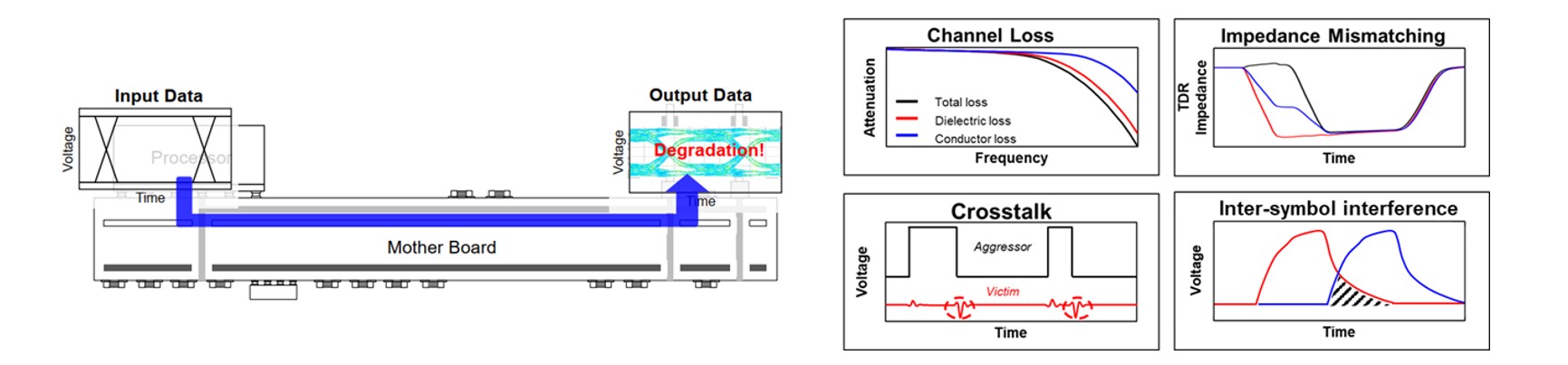
Signal Integrity Issue in High-Speed Channel
-
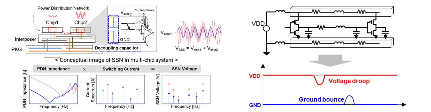
Power Integrity Issue in Package Structure
Signal integrity refers to the ability of a digital or analog signal to maintain its quality and integrity as it travels through a circuit or transmission medium. It involves preserving the signal's shape, amplitude, and timing, ensuring that the receiver can accurately interpret the transmitted information. In high-speed systems, factors like reflections, crosstalk, and noise can cause signal degradation, resulting in errors, timing issues, or even complete signal loss. Signal integrity analysis aims to understand and mitigate these issues through proper design techniques, including controlled impedance matching, transmission line routing, termination, and equalization.
Power integrity deals with the reliable delivery of power to integrated circuits (ICs) and other electronic components within a system. It focuses on maintaining a stable and noise-free power distribution network (PDN) to ensure that ICs receive the required voltage and current with minimal fluctuations and noise. Power integrity issues, such as excessive voltage drop, ground bounce, or power supply noise, can lead to functional failures, reduced performance, or even damage to the circuitry. Power integrity analysis involves evaluating the PDN's impedance profile, decoupling capacitors, power plane designs, and routing techniques to minimize power distribution problems and ensure proper power delivery.
Signal Integrity Modeling of Advanced Package Component-

Modeling of DRAM Package Component
-
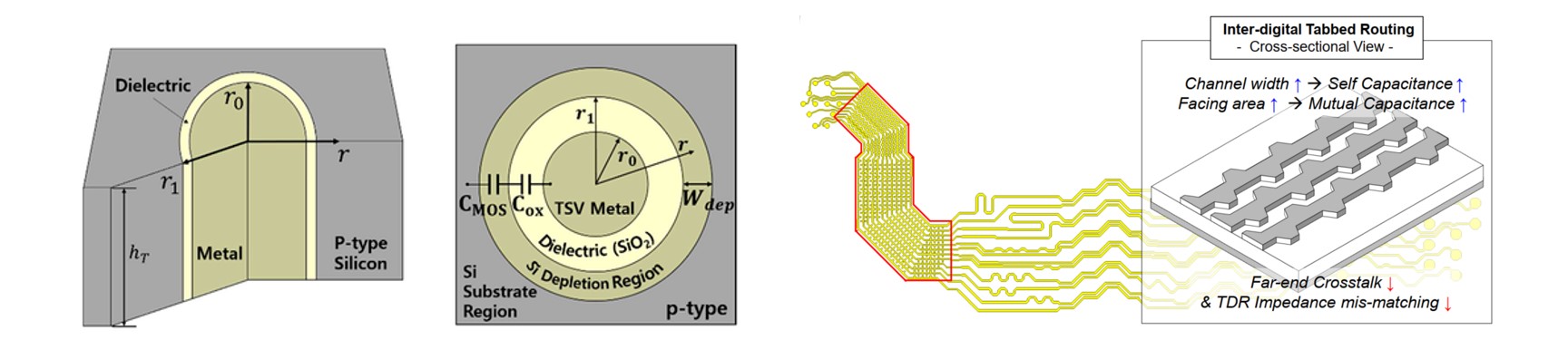
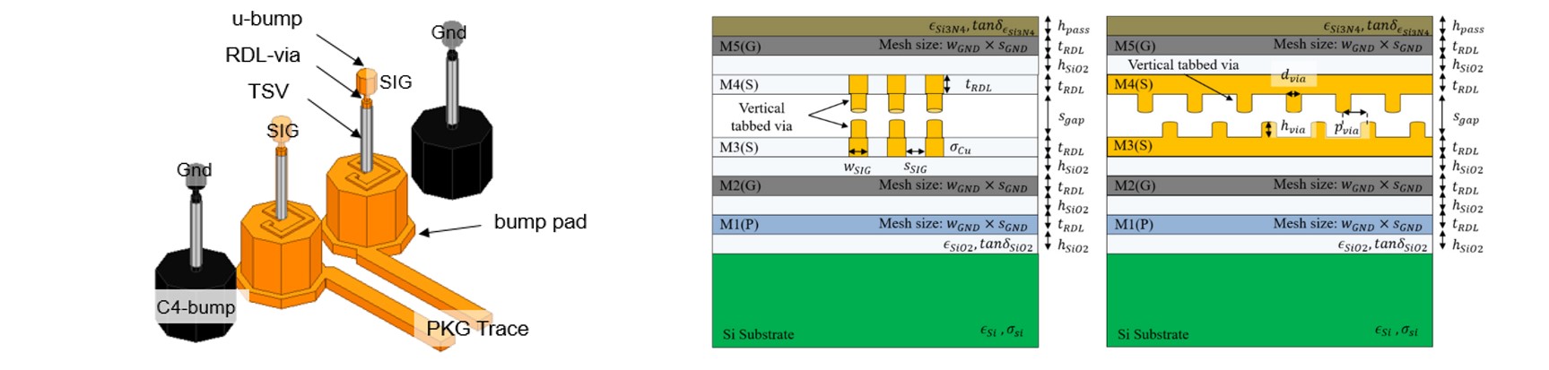
Signal Integrity Modeling of Through-silicon via(TSV) and Tab-Routing
Signal and power integrity modeling for packages, such as high-speed integrated circuits (ICs), system-in-package (SiP), multi-chip modules (MCM), and 3D-ICs, is crucial to ensure the reliable operation of high-speed circuits, minimize signal degradation, mitigate crosstalk and EMI. These modeling techniques enable designers to predict and address potential issues early in the design phase, reducing costly iterations and improving overall product performance and reliability. With increasing data rates and frequencies, signal integrity becomes critical to ensure that signals propagate correctly without distortion or degradation.
Signal integrity modeling helps identify and mitigate issues like signal reflection, crosstalk, ringing, and attenuation. By analyzing transmission line effects, impedance matching, and termination schemes, designers can optimize the package design to maintain signal quality and minimize signal integrity problems.
Channel Structure Design of High-Speed / Bandwidth System-
High Speed Channel Improvement through Impedance Compensation
-
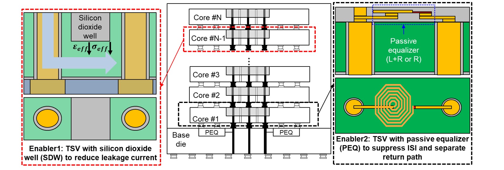
High Speed and Low Power Through-Silicon Via Enabler for HBM
The design of high-speed and high-bandwidth channels for advanced package is an essential technology for ensuring signal integrity (SI) of next-generation high-speed channels. As the data rates and channel densities increase, various signal integrity issues arise, such as channel loss, phase delay, impedance mismatching, and crosstalk. To address these serious signal integrity problems, novel channel structures are proposed and analyzed considering signal integrity and manufacture process with 3D-electromagnetic simulation and circuit simulation.
Through silicon via (TSV) with oxide well to reduce leakage current due to conductivity of silicon, a channel structure with vertical tabbed via to reduce crosstalk, and a compensation structure to reduce impedance mismatching were proposed and analyzed. These channel design techniques, the next-generation high-speed and high-bandwidth channels are designed.
AI-based Signal and Power Integrity Design-
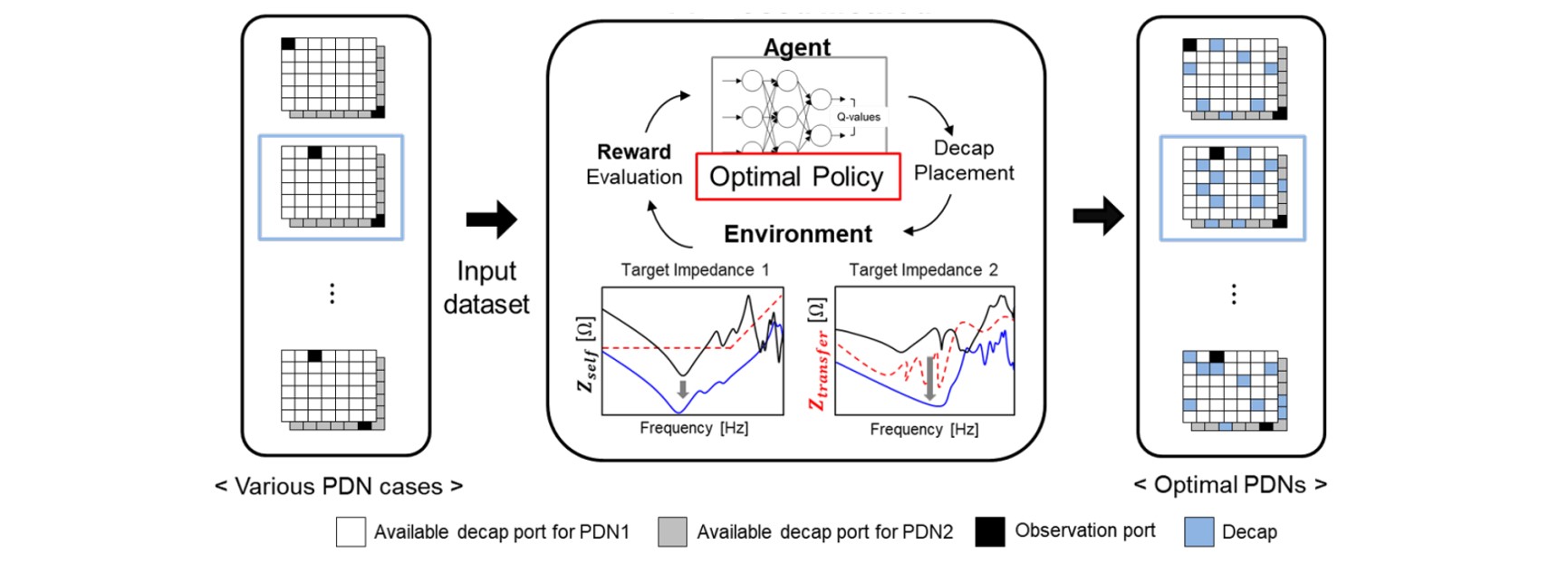
Decoupling Capacitor Optimization for Multi-Power Domain
-
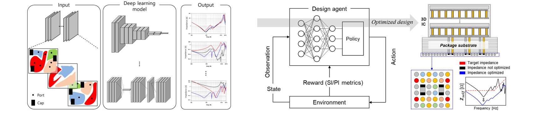
Power Integrity Optimization of Package Substrate for 3D-ICs
With the growth of the electronics industry, high-speed, wide-band, and small-sized electronic components development is required to process extensive amounts of information. These changes have been accelerated and developed into more complex, difficult signal and power integrity (SI & PI) problems such as massive coupling, power and signal interference. Newly occurring SI & PI problems must be analyzed and resolved for the next-generation electronic components. Artificial intelligence (AI) can be used to effectively solve these SI & PI problems.
First, it can replace measurements and simulations that require a long time and development. Through the ability of understanding the correlation between data, it is possible to immediately infer the performance of the electronic component by identifying the relationship between independent and dependent variables. This enable simple and quick system design and dramatically reduce the time required for product development. Second, a new optimal design method can be proposed considering the interaction of the entire system. Therefore, it is possible to propose a new global optimum design suitable for each environment and next-generation electronic parts.